|
Eddy current inspection is one of several NDT methods that use the principal of
"electromagnetism" as the basis for conducting examinations. Several other methods
such as Remote Field Testing (RFT), Flux Leakage and Barkhausen Noise also use this
principle.
Eddy currents are created through a process called electromagnetic induction. When
alternating current is applied to the conductor, such as copper wire, a magnetic
field develops in and around the conductor. This magnetic field expands as the alternating
current rises to maximum and collapses as the current is reduced to zero. If another
electrical conductor is brought into the close proximity to this changing magnetic
field, current will be induced in this second conductor. Eddy currents are induced
electrical currents that flow in a circular path. They get their name from "eddies"
that are formed when a liquid or gas flows in a circular path around obstacles when
conditions are right.
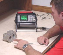
One of the major advantages of eddy current as an NDT tool is the variety of inspections
and measurements that can be performed. Eddy current measurements are very fast
and therefore have large applications for online testing of mass produced standard
components such as bars, screws, nuts, taps etc.
IIn the proper circumstances, eddy currents can be used for:
- Crack detection
- Material thickness measurements
- Coating thickness measurements
- Case depth determination
- Heat treatment monitoring
- Detection of ultra granular corrosion, pitting, inclusions of foreign metals etc.
Some of the advantages of eddy current inspection include:
- Sensitive to small cracks and other defects
- Detects surface and near surface defects
- Inspection gives immediate results
- Equipment is very portable
- Minimum part preparation is required
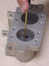
- Test probe does not need to contact the part
- Inspects complex shapes and sizes of conductive materials
|
|